Wafer-Level Optics
Coating Equipment for Precision Optical Components

Optical filter layers deposited directly on glass or semiconductor wafers enable optical products that have a very small size and a competitive price-performance ratio. Therefore, they have found their way into various markets such as consumer electronics or the automotive industry. Due to the increasing demand for high volume production, wafer-level optics are becoming the focus of the industry.

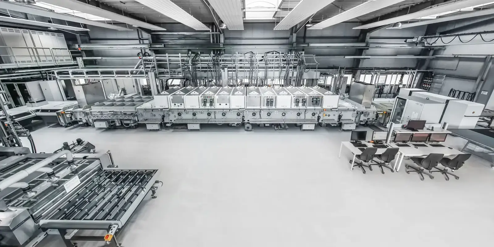
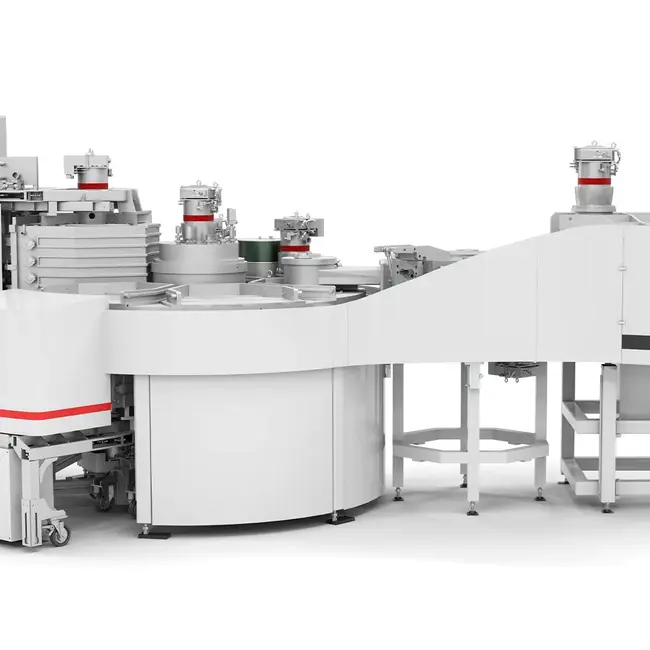
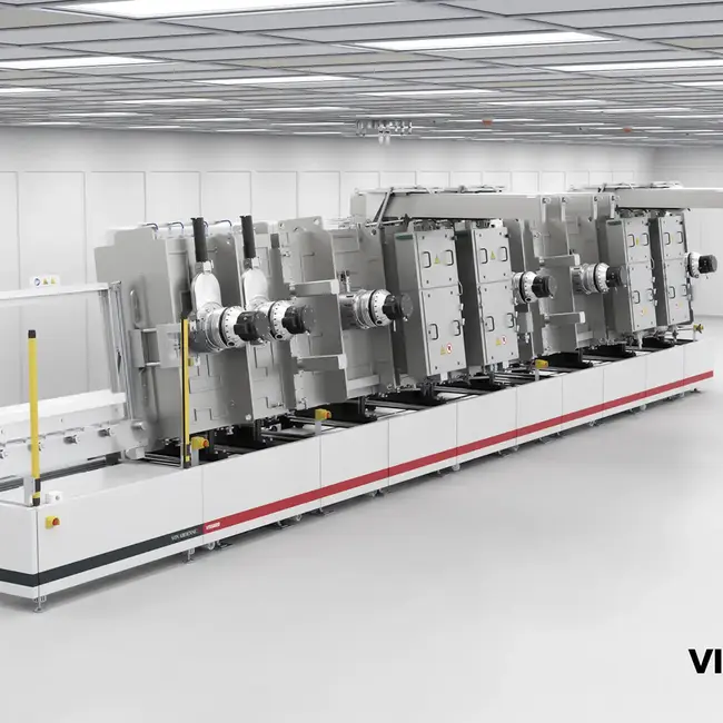
With the OPTA X, we offer you a coating system that has been specially developed to meet the requirements in the fields of photonics and wafer level optics.

For multilayer coating of wafer-based microlens arrays, semiconductor sensors or filter-on-chip CMOS, the OPTA X provides you with fully automated, SEMI-compatible wafer handling for integration in semiconductor fabs. In addition to wafers with a diameter of 200 millimeters, the OPTA X is also suitable for wafer sizes up to 300 millimeters.

Would you like to learn more? Then click on the content below or contact us directly.

Optical filter layers directly on glass and semiconductor wafers

 e.g. for silicon devices

Optical monitoring of transmission or reflection

directly on the wafer

SEMI-compatible wafer handling

for integration in semiconductor fabs

Support
Media
Successful kick off: Sustainability Network Dresden meets at VON ARDENNE

On November 22, 2022, VON ARDENNE hosted the first meeting of the Sustainability Network Dresden, which was launched on the initiative of the Dresden…

Digital Solutions for Resource Efficiency in Glass Coating

The recent discussion about climate neutrality and shifting the energy industry towards it is focusing on the development of renewable energy sources.…

Automated process stabilization for glass coating - with VA PROCESSMASTER

In this video, Harald Hagenström, vice president glass, introduces the VA PROCESSMASTER. This tool enables our customers to create complex and…

VON ARDENNE at the AVS 2022 - Key Takeaways

This video provides some insights into the AVS68 in Pittsburgh. Brian Cohen and Daniel Radach from VON ARDENNE North America talk about their…

Coating Equipment for Precision Optical Coatings

A crucial prerequisite for precision optics to function is high-precision coatings that make use of the interference properties and, thereby, provide…

What makes electron-beam assisted PVD coating so special?

The ability to coat a multitude of surfaces with specific materials is extremely important for providing technologies and products for our everyday…

Perovskite PV: Status, Importance and Manufacturing Technologies

Some say that solar energy is the new oil. And perovskite solar cells appear to be the latest technology trend in the industry offering a huge…

What is the most efficient way to melt refractory and reactive metals?

Refractory and reactive metals have extraordinary properties such as resistance to heat, corrosion, and wear. These are extremely interesting…

Magnetron Sputtering: How It Began and How VON ARDENNE Became a Technology Pioneer

What is extremely thin, almost invisible and transforms a piece of glass into a touch screen surface that is easy to clean? Or into a windshield that…

VIDEO: Future Trends in Photovoltaics | Cleantech Conversations

In this first episode of our new series Cleantech Conversations, we have interviewed Jonathan Gifford, Editor in Chief at pv magazine about future…

CONTACT
Trade fairs
25.04.2023 - 26.04.2023
OptecNet Fürstenfeldbruck 2023

Fürstenfeldbruck, Veranstaltungsforum

08.05.2023 - 11.05.2023
SVC Washington 2023

Booth: 420
Washington (DC), Gaylord National Resort & Convention Center

27.06.2023 - 30.06.2023
Laser World of Photonics 2023

Booth: B1/452
München, Messe

11.09.2023 - 15.09.2023
EOS Annual Meeting Dijon 2023

Dijon, Exhibition and Convention Center

19.09.2023 ä 21.09.2023
V2023

Dresden, Internationales Congress Center

Contact persons
Michael Schneider

Technical Sales Europe VON ARDENNE GmbH