
Support
Engineering
Simulation . Sampling . Layout
Technology & Application Center
Sampling . Development . Scaling
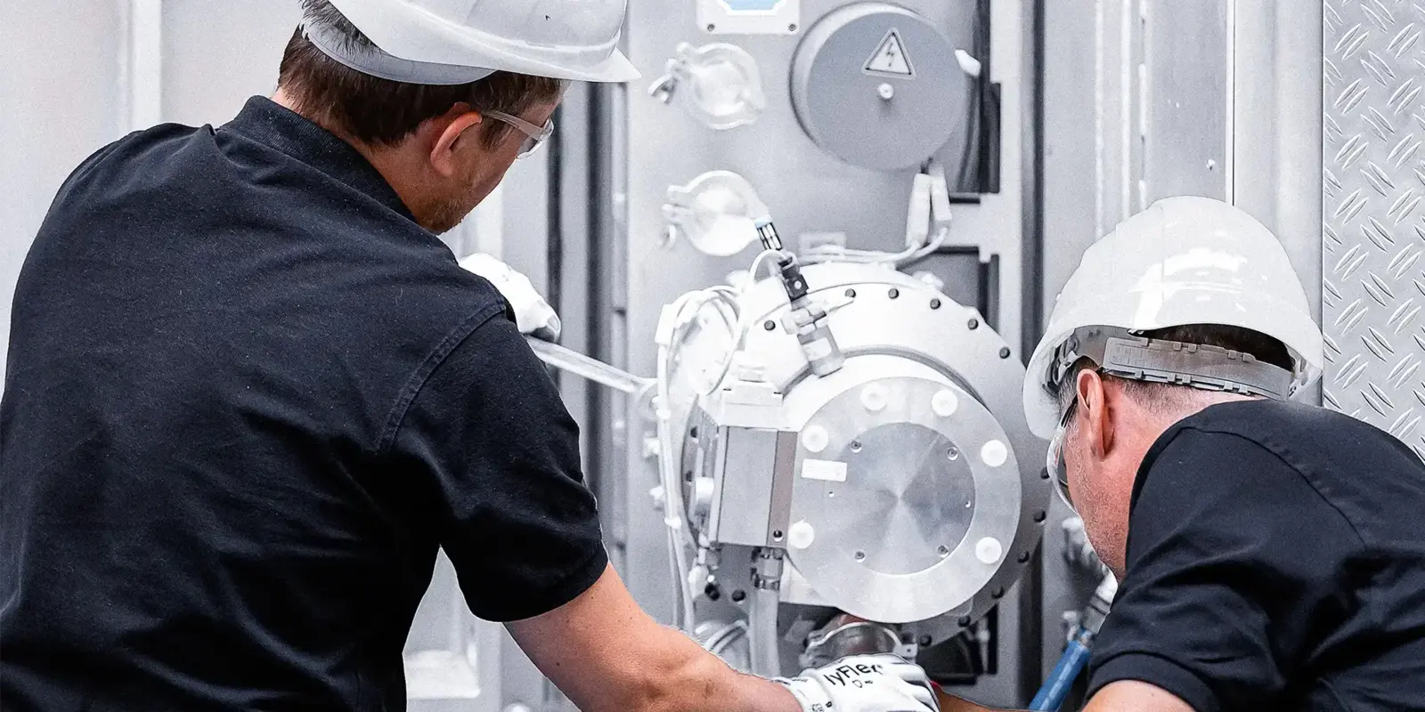
Service
Customer Portal . Spare Parts . Trainings
CONTACT
No news available.