OPTA X
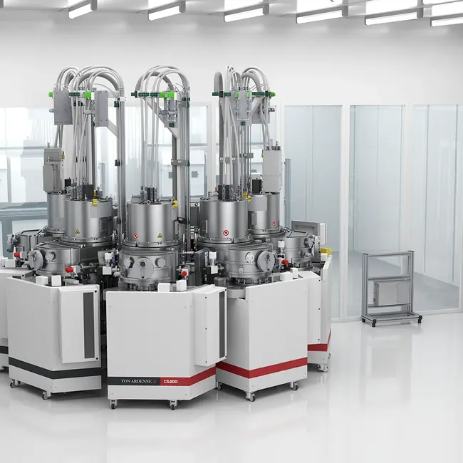
Rotary Disk Coating System

The OPTA X is a high­ly pro­duc­tive coa­ting sys­tem for mul­ti­lay­er stacks with a high num­ber of al­ter­na­ting, high-pre­ci­sion lay­ers. It is al­so suit­able for the pre­cise de­po­si­tion of sin­gle lay­ers of ox­ides, ni­trides and oth­er ma­te­ri­als. It de­liv­ers ex­cel­lent lay­er uni­for­mi­ties of typ­i­cal­ly ±0.25% and forms very thin, sin­gle-dig­it-na­nome­ter lay­ers as well as sev­er­al 100-na­nome­ter-thick lay­ers in mul­ti­lay­er stacks of the same or dif­fer­ent ma­te­ri­als.

The plat­form is suit­able for de­mand­ing op­ti­cal mul­ti­lay­ers made from sil­i­con di­ox­ide (SiO₂), nio­bi­um pen­tox­ide (Nb₂O₅), tan­ta­lum pen­tox­ide (Ta₂O₅), ti­ta­ni­um di­ox­ide (TiO₂), haf­ni­um ox­ide (HfO₂), hy­dro­gen­at­ed amor­phous sil­i­con (a-Si:H), and sil­i­con ni­tride (Si₃N₄), as well as emerg­ing semi­con­duc­tor ma­te­ri­als. These in­clude high-per­for­mance pi­e­zo­elec­tric ma­te­ri­als such as alu­mi­num ni­tride (AlN) and alu­mi­num scan­di­um ni­tride (Al₁₋ₓScₓN), as well as gal­li­um ox­ide (Ga₂O₃) and gal­li­um ni­tride (GaN) for wide-band­gap and ul­tra-wide-band­gap (WBG/UWBG) ap­pli­ca­tions.

The ro­ta­ry disk sys­tem can coat one or both sides of the sub­strate si­mul­ta­neous­ly in a hor­i­zon­tal ori­en­ta­tion, mak­ing the tool par­tic­u­lar­ly well suit­ed for stress-com­pen­sat­ed coat­ing of very thin or flex­i­ble sub­strates.

Read more

Be­cause no han­dling is re­quired be­tween in­di­vid­u­al de­po­si­tion steps, com­plex stacks com­pris­ing 5 to 1,000 lay­ers can be pro­duced. The OPTA X han­dles dif­fer­ent form fac­tors with di­am­e­ters or widths of up to 300 mil­li­me­ters. For op­ti­mal coat­ing re­sults, the pro­pri­e­tary Com­pound As­sist­ed Re­ac­tive Sput­ter­ing (CARS) and Me­ta Mode* tech­nol­o­gies are used. Both sput­ter­ing modes can de­liv­er high qual­i­ty Ox­ides at high rates of ap­prox­i­mate­ly 0.5 nm/s on full batch­es of, for ex­am­ple, 13 mm x 300 mm wafers or car­ri­ers. Re­ac­tive and non-re­ac­tive sput­ter­ing are al­so avail­able.

For max­i­mum flex­i­bil­i­ty, mag­ne­trons and/or plas­ma sources can be in­te­grat­ed at up to five po­si­tions per coat­ing side, and these po­si­tions can be equipped with dif­fer­ent ma­te­ri­als. In-si­tu mea­sure­ment tech­nol­o­gy is avail­able for op­ti­cal mon­i­tor­ing and can be used for in­line pro­cess con­trol to op­ti­mize op­ti­cal fil­ters in re­al time based on phys­i­cal mod­el­ing dur­ing the coat­ing pro­cess.

The OPTA X is equipped with an au­to­mat­ic, mod­u­lar trans­fer sys­tem for the safe load­ing of dif­fer­ent sub­strates. The semi­con­duc­tor ver­sion of the OPTA X al­lows for full OHT au­to­ma­tion and sub­strate trans­fer from SMI­Fs and FOU­Ps, while the op­tics ver­sion uses adapt­able car­ri­ers for flex­i­bil­i­ty and mul­ti-load lock cham­bers for par­ti­cle re­duc­tion and high pro­duc­tiv­i­ty dur­ing mul­ti­ple unat­tend­ed de­po­si­tion batch­es.

*
The CARS mode com­bines mag­ne­tron sput­ter­ing from ce­ram­ic tar­gets with an RF-ICP plas­ma pro­cess. Dur­ing each ro­ta­tion, a sub-stoi­chio­met­ric ox­ide or ni­tride mon­o­lay­er is de­pos­it­ed and sub­se­quent­ly ful­ly ox­i­dized or ni­tri­dized to form a stoi­chio­met­ric lay­er.

The Me­ta Mode us­es a met­al tar­get in the mag­ne­tron sput­ter­ing com­part­ment and an RF-ICP plas­ma pro­cess for sub­se­quent ox­i­da­tion or ni­tri­da­tion. A thin me­tal­lic lay­er is de­pos­it­ed in the mag­ne­tron sput­ter­ing com­part­ment and then ful­ly re­act­ed in the RF-ICP plas­ma zone. This keeps the met­al tar­get clean and avoids the con­ven­tion­al tar­get-poi­son­ing is­sue.

Would you like to learn more? Explore the content below or contact us.

Highest precision & quality

through fast, clean, low-defect, homogeneous coatings

Anti-warp effect

through double-sided deposition with different materials

Variable product adaptation:

layers, layer systems & component geometry

OPTA X200
  • Optimized for applications on substrates with diameters of up to 200 mm
  • Meets the highest demands in optical applications through highly pure and defect-free optical layers
  • Unique homogeneity and chemical composition of the electrical layers for optimal results in microelectronics and the semiconductor industry
OPTA X300
  • Processing substrates with diameters of up to 300 mm, including G12 wafers
  • Meets the highest demands in optical applications through highly pure and defect-free optical layers
  • Unique homogeneity and chemical composition of the electrical layers for optimal results in microelectronics and the semiconductor industry
Details

Technical Data

 OPTA X200OPTA X300
Optical applicationsOptical windows and filters, dielectric mirrors, displays, wafer-level optics, AR/VR*
Semiconductor applicationsMEMSadvanced packaging, photonics
Coating materialsSiO2, Al2O3, Nb2O5, Ta2O5, TiO2, HfO2, Si3N4, ITO, Al, Ag, AlScN, AlN, multilayers
Technologiesdouble-sided coating without flipping, CARS, Meta Mode, reactive sputtering, planar/rotatable cathodes
Deposition modesdirect current (DC), pulsed direct current (pulsed DC), radio frequency (RF)
Process monitoringMOCCA+*
Process stationsup to 8 rotatable dual magnetrons (RDM), 2 RF plasma sources
Magnet systemsadjustable*
Substrate materialssilicon, glass, metals, polymers*
Substrate diameter200 mm300 mm
TemperatureRT up to 300 °C*
Capacity12 pcs.13 pcs.
Rotation speed1–250 rpm*
Software & controlSiemens PLC SIMATIC and WinCC*

*applies to both system types

CLEANROOM
  • Manufacturing of vacuum coating systems
  • Sampling & pilot deposition services
  • 600 m² semiconductor cleanroom including AMC capability
Support
Media
New SKYVA2000 Vacuum Coating System for Large-Aperture Optics

Proven technology behind the Vera C. Rubin Observatory and the Gran Telescopio Canarias supports next-generation terrestrial observation and space-…

Beyond Silicon Carbide & Gallium Nitride —on Gallium Oxide & the Case for PVD

Aalyia Shaukat of Power Electronics News interviews Guido Überreiter, VP of Semiconductor Strategy at VON ARDENNE, a German vacuum coating equipment…

VON ARDENNE Commissions New Deposition Tool OPTA X300 in Cleanroom

VON ARDENNE is commissioning its new deposition tool, the OPTA X300, in its recently opened cleanroom in Germany. The OPTA X300 enables the production…

Transitioning Advanced Packaging from More Moore to More than Moore

For decades, the semiconductor industry has pursued a clear objective: to integrate as many functions as possible into a single system-on-chip (SoC).…

VON ARDENNE Unveils New Cleanroom at Headquarters

State-of-the-art facility for sampling, assembly and commissioning

New OPTA X300 Deposition Tool & New Cleanroom

Company showcases its advanced engineering capabilities and new deposition solutions at SEMICON West

A New Era in Astronomy - with VON ARDENNE Technology

On June 23, 2025, the Vera C. Rubin Observatory presented the first results of its work with the Large Synoptic Survey Telescope (LSST). About 14…

VON ARDENNE Group presents unique technology package at Laser World of Photonics 2025

Broad technology portfolio with ion beam and plasma processes and equipment for the precise coating and structuring of surfaces

Mirror on the mountain: Milestone at Rubin Observatory

Successful reflective coating of the 8.4-meter primary/tertiary mirror with VON ARDENNE coating system:

Unique technology package for optical coatings

Bundled strength: VON ARDENNE Group presents unique technology package for optical coatings at Optatec 2024


There are only a few providers of…

CONTACT
13.10.2026 - 15.10.2026
Semicon West 2026

San Francisco, CA, USA

Moscone Center

North Hall | Booth 5373

18.11.2026 - 21.11.2026
Semicon Europe 2026

Munich, Germany

Exhibition Center

C2 / C2317

Michael Schneider

Vice President Semiconductors & Precision Optics I Space & AviationVON ARDENNE GmbH

Search