CLUSTER SYSTEMS
for Research, Develop­ment & Production

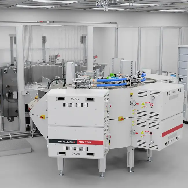
Our clus­ter sys­tems are mo­du­lar coa­ting sys­tems sui­ta­ble for high­ly fle­xi­ble and high­ly pro­duc­ti­ve pro­ces­ses in the de­ve­lop­ment and pro­duc­tion of se­mi­con­duc­tors, op­tics, or in pho­to­vol­ta­ic ap­pli­ca­ti­ons. They are spe­ci­fi­cal­ly de­si­gned for pro­ces­sing sub­stra­tes with a dia­me­ter or wi­dth of up to 300 mil­li­me­ters.

This ma­kes them ide­al for de­ve­lo­ping new coa­ting tech­no­lo­gies and for pro­du­cing lay­ers or stacks with dif­fe­rent ma­te­ri­als, tai­lo­red pro­per­ties, high pre­ci­si­on, and ex­cel­lent re­pro­du­ci­bi­li­ty.

Ty­pi­cal ap­pli­ca­ti­ons in­clu­de MEMS, wi­de-band­gap or ul­tra-wi­de-band­gap (WBG/UWBG) de­vi­ces and through-si­li­con vi­as (TSVs) for 3D ad­van­ced-pack­a­ging ap­pli­ca­ti­ons in the se­mi­con­duc­tor in­dus­try, as well as stan­dard con­duc­ting or in­su­la­ting lay­ers. Clus­ter sys­tems can al­so be used to de­ve­lop next-ge­ne­ra­ti­on so­lar cells such as TOP­Con and pe­rov­skite tan­dem.

Read more

Thanks to their great fle­xi­bi­li­ty, the clus­ter sys­tems of­fer low ope­ra­ting costs. Each sys­tem can be con­fi­gu­red to your spe­ci­fic tasks: up to se­ven pro­cess cham­bers and one or mo­re load locks can be ar­ranged around the cen­tral trans­fer cham­ber. All cham­bers are se­pa­ra­ted from each other in terms of both va­cu­um tech­no­lo­gy and con­trol sys­tems, al­lo­wing pro­ces­ses to be per­for­med in­de­pen­dent­ly and si­mul­ta­ne­ous­ly.

Sub­stra­tes are trans­fer­red from SMI­Fs, FOU­Ps or load locks di­rect­ly through the sys­tem or in ad­ap­tab­le car­ri­ers.

Would you like to learn more? Explore the content below or contact us.

Scalable

through modular design

Adapted to your needs

through flexible configuration

Helps you reduce operating costs

through flexibility

CS200
  • Ideal for applications in the semiconductor and optics industries
  • High throughput
  • Compact dimensions
CS300
  • Ideal for applications in the semiconductor, optics, and PV industries
  • Optimized for R&D and production of TOPCon and perovskite tandem solar cells
CLEANROOM
  • Manufacturing of vacuum coating systems
  • Sampling & pilot deposition services
  • 600 m² semiconductor cleanroom including AMC capability
Support
Media
Customer Portal "myVA" Now Available

It's here: the myVA Customer Portal. VON ARDENNE has developed it with the aim of simplifying interactions, providing valuable insights and increasing…

Transitioning Advanced Packaging from More Moore to More than Moore

For decades, the semiconductor industry has pursued a clear objective: to integrate as many functions as possible into a single system-on-chip (SoC).…

CONTACT
13.10.2026 - 15.10.2026
Semicon West 2026

San Francisco, CA, USA

Moscone Center

North Hall | Booth 5373

22.10.2026 - 24.10.2026
REI India 2026

Greater Noida, India

India Expo Mart

German Pavillon

18.11.2026 - 21.11.2026
Semicon Europe 2026

Munich, Germany

Exhibition Center

C2 / C2317
SALES Contact

Am Hahnweg 8
01328 Dresden
Germany

Search